The BK3432 chip is a highly integrated Bluetooth 5.0 dual mode data SoC with 2 Mbit/s data rate supported. It integrates a high-performance RF transceiver, baseband, MCU, rich feature peripheral units, programmable protocol and profile to support Bluetooth classic and low energy application. The Flash program memory makes it suitable for customized applications.
The BK3432 is designed with advanced technology process and integrated with switch DCDC regulator, that it has ultra-low power consumption and ultra-low leakage power. The embedded high order interference suppression filter and fast automatic gain control logic make it work well in high interference environment.
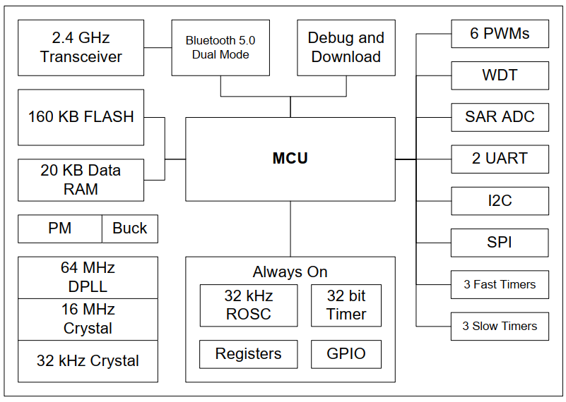
The following figure illustrates the BK3432 Block chip:
The following figure illustrates the BK3432 QFN32 pin assignment.
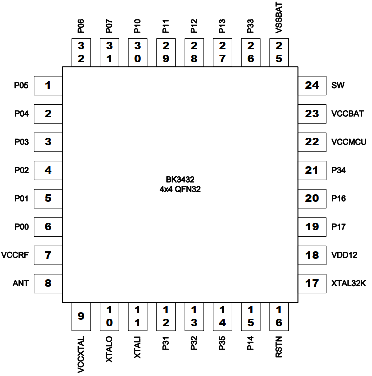
The following table describes the BK3432 QFN32 pins.
| Pin | Name | Pin function | Description |
|---|---|---|---|
| 1 | P05 | Digital I/O | General purpose IO |
| 2 | P04 | Digital I/O | General purpose IO |
| 3 | P03 | Digital I/O | General purpose IO |
| 4 | P02 | Digital I/O | General purpose IO |
| 5 | P01 | Digital I/O | General purpose IO |
| 6 | P00 | Digital I/O | General purpose IO |
| 7 | VCCRF | Power | RF power, 1.5 V |
| 8 | ANT | RF | RF signal port |
| 9 | VCCXTAL | Power | Crystal power, 1.5 V |
| 10 | XTALO | Analog | 16 MHz crystal output |
| 11 | XTALI | Analog | 16 MHz crystal input |
| 12 | P31 | Digital I/O | General purpose IO |
| 13 | P32 | Digital I/O | General purpose IO |
| 14 | P35 | Digital I/O | General purpose IO |
| 15 | P14 | Digital I/O | General purpose IO |
| 16 | RSTN | Analog | Active low pin reset |
| 17 | XTAL32K | Analog | 32 kHz Crystal input |
| 18 | VDD12 | IAnalog | LDO output, 1.5 V |
| 19 | P17 | Digital I/O | General purpose IO |
| 20 | P16 | Digital I/O | General purpose IO |
| 21 | P34 | Digital I/O | General purpose IO |
| 22 | VCCMCU | Power | Power, 1.5 |
| 23 | VCCBAT | Analog | Power, 3 V |
| 24 | SW | Analog | Switch regulator pin for two battery mode |
| 25 | VSSBAT | Analog | Ground |
| 26 | P33 | Digital I/O | General purpose IO |
| 27 | P13 | Digital I/O | General purpose IO |
| 28 | P12 | Digital I/O | General purpose IO |
| 29 | P11 | Digital I/O | General purpose IO |
| 30 | P10 | Digital I/O | General purpose IO |
| 31 | P07 | Digital I/O | General purpose IO |
| 32 | P06 | Digital I/O | General purpose IO |
The BK3432 QFN32 has totally 20 GPIO pins, which can be configured as either input or output. There are secondary functions available for GPIO pins and configurable by firmware.
At the beginning of the chip starts up, the chip will enter programming mode, JTAG mode or normal according received command from Mode Selecting Pin.
The following table describes the BK3432 GPIO function mapping.
| No. | Description | I/O | Program mode | Mode selection pin | JTAG mode |
|---|---|---|---|---|---|
| P00 | UART_TX | O | |||
| P01 | UART_RX | I | |||
| P02 | I2C_SCL | I/O | |||
| P03 | I2C_SDA | I/O | JTAG_NTRST | ||
| P04 | SPI_SCK | I/O | SPI_MOSI | SPI_MOSI | JTAG_TDI |
| P05 | SPI_MOSI | I/O | SPI_MISO | SPI_MISO | JTAG_TDO |
| P06 | SPI_MISO/PWM[4] | I/O | SPI_SCK | SPI_SCK | JTAG_TCK |
| P07 | SPI_NSS/PWM[5] | I/O | SPI_CS | SPI_CS | JTAG_TMS |
| P10 | PWM[0] (20mA) | O | |||
| P11 | PWM[1] (20mA) | O | |||
| P12 | PWM[2] | O | |||
| P13 | PWM[3] | O | |||
| P14 | PWM[4] | ||||
| P16 | UART2_TX | O | |||
| P17 | UART2_RX | O | |||
| P31 | Ch1 | I | |||
| P32 | Ch2 | I | |||
| P33 | Ch3 | ||||
| P34 | Ch4 | I | |||
| P35 | Ch5 | I |
Each GPIO pin can be the source to wake up MCU from shut down state. In the shutdown state, any voltage level change on the pre-configured GPIO pin will trigger the wake-up procedure.
PWM timers
There are six 16 bits PWM timers. The clock of PWM timers can be selected as 32 KHz clock or 16 MHz clock by register.
There are two modes of PWM timers. One is timer mode and another is PWM mode. The timer mode can generate interrupt to MCU. The PWM mode can generate PWM waveform and output to GPIO pins to drive external device such as LED. Six GPIO pins can be used to output PWM waveform separately.
Watch dog timer and RTC timer
The watch dog timer and RTC timer run on the always on power domain, whose clock source is 32 kHz clock.
The 16 bits watch dog timer runs with 4 kHz frequency that its period can be up to 16 second. After watch dog timer is expired, it will reset the whole chip.
The 32 bits RTC timer in always on power domain run with ROSC frequency that its period can be up to one day. After RTC timer is expired, it will wake up the MCU.
A 10-bit generic ADC is integrated in BK3432. Total five external channels and one internal channel can be selected for ADC transfer. It supports both single and continuous mode.
| ADC channel number | ADC source |
|---|---|
| Channel 1 | GPIO31 |
| Channel 2 | GPIO32 |
| Channel 3 | GPIO33 |
| Channel 4 | GPIO34 |
| Channel 5 | GPIO35 |
| Channel 7 | VCCBAT-pin |
There are two set UARTs, one set I2C and one set SPI interface, which support both master and slave mode.
The UART baud rate can be up to 3.2 MHz, and the SPI clock speed can be up to 4 MHz。
There is a true random number generator to make system get better security communication.
The FLASH content will be protected (not readable, but erasable) as long as the LSB bit 3 or bit 5 of the last 32-bit word of last address 0x9FFF is set to zero.
The following table describes the BK3432 RF characteristics:
| Name | Parameter(Condition) | Min | Typical | Max | Unit | Comment |
|---|---|---|---|---|---|---|
| VCC | Voltage | 0.9 | 3.0 | 3.6 | V | |
| TEMP | Temperature | —40 | +27 | +125 | ºC | |
| VIH | High level | VCC-0.3 | VCC+0.3 | V | ||
| VIL | Low level | VSS | VSS+0.3 | V | ||
| VOH | High level (IOH=-0.25mA) | VCC- 0.3 | VCC | V | ||
| VOL | Low level(IOL=0.25mA) | VSS | VSS+0.3 | V | ||
| IVDD | Deep sleep | 0.5 | uA | |||
| IVDD | Sleep current (RF OFF,32kHz clock,DIG Retention | 1.8 | uA | |||
| IVDD | Active RX (3.3 V) | 5.1 | mA | With DCDC regulator | ||
| IVDD | Active TX @ -1 dBm (3.3V) | 4.8 | mA | With DCDC regulator | ||
| FOP | Operating frequency | 2400 | 2480 | MHz | ||
| FXTAL | Crystal frequency | 16 | MHz | |||
| RFSK | Air data rate | 1 | 2 | Mbps | ||
| PRF | Output power | -20 | —1 | +4 | dBm | |
| PBW | Modulation 20 dB bandwidth | 1 | MHz | |||
| PRF1 | Out of band emission 2 MHz | —20 | dB | |||
| PRF2 | Out of band emission 3 MHz | —58 | dB | |||
| Dev | Transmit FM deviation | 115 | 250 | 300 | kHz | |
| Drift | Transmit drift in any position | 400 | Hz/us | |||
| Max Input | 1 E-3 BER | -10 | dBm | |||
| RXSENS | 1 E-3 BER sensitivity | -96 | -97 | dBm | ||
| Intermo dulation | Pin=-64 dBm; Punwant=- 50 dBm; f0=2f1-f2, f2- f1=3 MHz or 4 MHz or 5MHz | -25 | -22 | dBm | ||
| C/ICO | Co-channel C/I | 7 | dB | |||
| C/I1ST | ACS C/I 1MHz | —9 | —6 | dB | ||
| C/I2ND | ACS C/I 2MHz | -44 | dB | |||
| C/I3RD | ACS C/I 3MHz | -50 | dB | |||
| C/I1STI | ACS C/I Image channel | -25 | dB | |||
| C/I2NDI | ACS C/I 1 MHz | -35 | dB | |||
| Block | Block @ 2399,and 2484 | -15 | dBm | |||
| Block | Block @ 2 GHz and 3 GHz | -15 | dBm | |||
| Leakage | Leakage @ < 1GHz | -71 | dBm | |||
| Leakage | Leakage @ >1GHz | -56 | dBm |
The BK3432 32-Pin uses the 4mmx4mm QFN package.
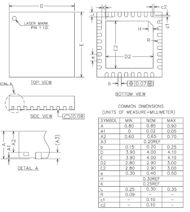
| Part number | Package | Packing | Minimum order quantity |
|---|---|---|---|
| BK3432QN32C | QFN 4mmx4mm 32-Pin | Tape Reel | 3K |
| Version | Date | Description |
|---|---|---|
| 0.1 | 12/Mar/2017 | The initial release. |
| 0.2 | 11/Nov/2018 | Modified the order information. |