CBU Module
This topic describes the relevant information you need to know for the hardware development of the CBU module.
Application scope
CBU is a low power embedded Wi-Fi module developed by Tuya Smart. It is composed of a highly integrated radio-frequency identification (RFID) chip BK7231N and a few peripheral components and supports dual connection of AP and STA as well as BLE connection.
Features
- Built-in with a low power 32-bit CPU, a 256 KB RAM, and a 2 MB flash.
- The basic frequency can be up to 120 MHz
- Support the complete functions of 802.11b/g/n
- Integrate the classical BLE system
- The maximum output power of +17 dBm in the 802.11b mode
- The maximum transmission power of 20 dBm in the Bluetooth mode
- Support three pairing mode including SmartConfig (EZ), AP, and BLE (available for the Android and iOS device)
- Either the PCB antenna or the FPC antenna will do
- The PCB onboard antennas with a peak gain of 2.5 dBi
- Operating voltage: 2.1V–3.6V
- Operating temperature: -40°C–105°C
For more information, see CBU Module Datasheet.
The minimum system circuit
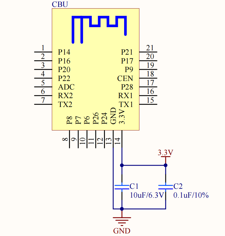
Things to note
Power supply designs under different working modes
| Working mode |
Working status, Ta=25°C |
Average value |
Maximum value (typical value) |
Unit |
| Bluetooth pairing status |
The module is in quick pairing status with the Wi-Fi indicator flickering quickly |
88 |
130 |
mA |
| AP pairing status |
The module is in access point pairing status with the Wi-Fi indicator flickering slowly |
95 |
180 |
mA |
| EZ pairing status |
The module is in quick pairing status with the Wi-Fi indicator flickering quickly |
90 |
168 |
mA |
| Connected |
The module is connected to the network with the Wi-Fi indicator always on |
90 |
134 |
mA |
RF power consumption
| Working status |
Mode |
Rate |
Transmission power/Receive |
Average value |
Peak value (typical value) |
Unit |
| Transmitting |
11b |
11 Mbit/s |
+17 dBm |
180 |
304 |
mA |
| Transmitting |
11g |
54 Mbit/s |
+15 dBm |
95 |
280 |
mA |
| Transmitting |
11n |
MCS7 |
+14 dBm |
101 |
273 |
mA |
| Receiving |
11b |
11 Mbit/s |
Continuously receiving |
73 |
76 |
mA |
| Receiving |
11g |
54 Mbit/s |
Continuously receiving |
75 |
78 |
mA |
| Receiving |
11n |
MCS7 |
Continuously receiving |
75 |
78 |
mA |
- The maximum working power consumption of the module is 3.3V/180 mA, and the maximum transient current of the transmitting (TX) is 304 mA. Considering the high-current charging upon the cold start of the large electrolytic capacitor of the peripheral power terminal, it is recommended to select a power supply with a stable power of ≥3.3V/220 mA and the peak current limit of ≥400 mA. The power consumption of other components must be considered when selecting a power supply in the whole product design.
- Power filter capacitors C1 and C2 shall be arranged near the power supply pin.
- Special I/O port description
- ADC pin: The detected voltage range is 0–2.4V and the conversion precision is up to 10 digits.
- The corresponding pins for the peripheral UART1 are RX1 and TX1. The pins are user serial ports by default, as well as firmware programming ports that can be configured to be general I/O ports.
- The corresponding pins for the peripheral UART2 are RX2 and TX2. The pins are log printing ports by default. They can be configured to be general I/O ports. Nevertheless, it is recommended not to use the peripheral UART2 for other functions when there are sufficient pins.
- The peripheral PWM and the 5-way stand-alone hardware can be configured to be a regular I/O port. The corresponding pins for the peripheral PWM are P6, P7, P8, P24, and P26.
- Reset pin CEN with pull-up resistor built-in. When not in use, the pin can float.
Antenna clearance description
Things to note
- Avoid using metal shells and shells with metallic paint or coating in the direction of the antenna radiation. Avoid using metal screws, metal rivets, or other metal parts that affect the antenna radiation.
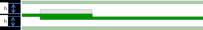
- The distance from the top cover to the antenna affects the antenna performance. The farther the shell is from the antenna, the less effect it has on the performance.
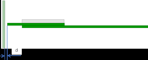
- The distance from the top-and-bottom shell to the antenna affects the antenna performance. The farther the shell is from the antenna, the less effect it has on the performance.
- Keep the module from horns, power switches, cameras, HDMI, USB, and other high-speed signals to avoid interference.
- Avoid metal shielding near the antenna. If there is co-channel interference, it is necessary to fully evaluate and ensure the isolation.
Placement
- Horizontal placement
It is recommended to place the module at the edge of the backplane with the antenna facing outward, and flush the module GND with the backplane GND that are fully connected with each other.

- Embedded placement
Embed the module to the backplane with a slot flushing with or deeper than the module ground. The side of the slot shall be ≥15 mm from the module board edge. A wider slot can achieve better performance but weaker than that of horizontal placement. 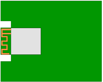
- Vertical placement
Insert the module into the backplane slot vertically with the antenna facing upward. The module GND and the backplane GND shall be fully connected with each other. In an ideal condition, the clearance around the antenna is ≥15mm.
RF test items and indicators
Since the antenna is susceptible to the distance from the shell to the surrounding components, it is recommended to test the RF performance after the whole device test. The RF test items and indicators are listed in the table below.
| Serial number |
Test item |
Test indicator |
| 1 |
Indoor distance increasing |
≥25m |
| 2 |
Outdoor distance increasing |
≥75m |
| 3 |
Total radiated power (TRP) of whole device signaling mode (11B 1 Mbit/s test mode) |
≥10 dBm |
| 4 |
Whole device TIS |
≤-62 dBm |
Note:
- Items 3 and 4 shall be tested in the dark chamber of the antenna manufacturer or certification authorities.
- The test items apply to most Wi-Fi products excluding certain special products.